Introduction
While it appears that we are nearing the sunset of Moore’s Law, we are still in for some incredible last acts in transistor size reduction and semiconductor manufacturing efficiency. With roots reaching back to the mid-1980s, atomic layer deposition has long been considered a potential route in semiconductor manufacturing that could allow Moore’s Law to continue unabated. The method of ALD sees the depositing of thin films of materials onto surfaces one atomic layer at a time, allowing for better control over film thickness and composition than traditional techniques.
The ALD process also enables smaller features and faster production rates, both of which are essential to meet increasing demand for more powerful consumer electronics. ALD could have huge implications on future semiconductor production, as the method should help manufacturers create faster devices that perform better, at an affordable cost. Moore’s Law should be allowed to prevail here, at least in the short term. And while the computer industry has thus far followed Moore’s vision generally, even Moore himself, who recently passed away at the age of 93, stated that there is an eventual limit and that he sees his law being overturned sometime in the 2020s.
The challenge of following Moore’s Law
The issue is that the high operating temperature of transistors eventually will make going smaller impossible, as cooling the transistors will take more energy than is passing through them. In a 2005 interview, Moore stated, “... the fact that materials are made of atoms is the fundamental limitation, and it's not that far away ... We're pushing up against some fairly fundamental limits, so one of these days, we're going to have to stop making things smaller.”

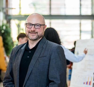
him earn his Ph.D. Image: Konner Holden
Today we get an inside look at ALD from an interview with Konner Holden, a process engineer at Lam Research who earned his undergraduate and doctoral degrees from Oregon State University. Engaged in research on ALD and how it can be used for stacking/multilayer chip design, Konner first shared his academic and professional journey, his industry partnership through research at Oregon State, and finally his current work on ALD at Lam. Collaborations among academia and industry, a staple of graduate engineering programs at Oregon State, allow for mutually beneficial scenarios in which research is advanced and great hires can be made.
Getting his start in computer science and then switching to electrical engineering, Holden excelled at Oregon State as an undergraduate student, noting that he took a “deep dive into how computers work, looking at transistors, really just the heart of everything.” Staying at Oregon State for graduate school, Holden began his research into ALD under the tutelage of his advisor, John Conley, professor of electrical and computer engineering and materials science. Here Holden stated that he “began using ALD to fabricate novel electronic devices and test new materials along with new ALD processes.”
When asked why he stayed on at Oregon State for his Ph.D, Holden said, “I felt that I’d already found my home. On top of that, I had access to the Materials Synthesis and Characterization Facility at Oregon State, and there was a great clean room environment. I felt I had everything I needed and didn’t feel any reason to go anywhere else or honestly even look anywhere else.” Holden's passion for research into ALD was unabated, and he didn't miss a beat.

one of the devices Holden fabricated as part of his work
with RedWave. The dots in the image are single atoms.
Image: Konner Holden
When asked about the arc of his postgraduate research, how he began working collaboratively with industry, and how this led to his current position at Lam, Holden explained, “First, Oregon State is highly collaborative. Not only is it geographically close to the Silicon Forest, Intel, and the like, but there are many collaborative research opportunities.” He added, “Red Wave Energy was one big supporter of my graduate school career. They’re a small startup in Colorado, and they helped fund much of my work. While collaborating with Red Wave, I was working on these new devices that could enable a new type of energy harvesting technology. I really enjoyed the work. Next, On Semiconductor sponsored some of my research work, and I even interned there twice, for two summers, which was a great experience. Those collaborations were significant in setting me up to get my foot in the door at Lam Research, where I am working full-time now in a process engineering group focused on ALD. Lam truly appreciated that I had this prior industry experience.”
Holden’s work in ALD at Lam started collaboratively in the second-to-last year of his grad school career at Oregon State. His advisor was already involved in the ALD community and was contacted by a technical director from Lam. On offer was a small grant from Lam called an “unlock ideas project.” The goal was to procure process engineers, like Holden, to explore new ideas that were somewhat "out there," as Holden noted, and not necessarily consumer-focused. With the recommendation and endorsement of his advisor, Holden slotted in nicely at Lam and began his deeper dive into ALD applications.

with a high-intensity ultraviolet light turned on. Holden
constructed this ultraviolet light source modification for
the reactor during the last year of his Ph.D. as part of
the Unlock Ideas project with Lam. Image Courtesy:
Konner Holden
When asked about his specific work in ALD at Lam Research, Holden stated, “I am currently working on a project at Lam related to packaging. A new development in this field is stacking chips together multiple layers deep, which would increase the number of devices that can be packed onto one single chip. The technology I’m researching could potentially make it easier for people to achieve this kind of stacking.” Holden added, “My work focuses on using the ALD approach, which could provide unique advantages in terms of material synthesis for these types of multilayer chip designs.”
With his research at Lam, Holden is part of what’s keeping Moore’s Law on the books, at least for now. With ALD in the wings and the advent of transistor size reduction, stacking, and efficiencies in semiconductor materials and manufacturing to follow, we should see some fantastic progress in the years to come. Yet the most significant takeaway here for industry is awareness of the collaborative opportunities to advance research and secure bright, young minds to expand the workforce. Oregon State’s highly collaborative nature, top facilities, and excellent geographic location make it an ideal partner in these realms. With today’s technology fast becoming only a reference point, industry and academia can stay ahead of the competition by working together.
To explore collaborative opportunities, or the semiconductor program in general, get in touch with us at: semi-osu@oregonstate.edu.