Introduction
The College of Engineering is leading efforts to build a sustainable semiconductor ecosystem in the Pacific Northwest
Oregon State University’s College of Engineering has been at the heart of the Silicon Forest for decades. That hub of microchip manufacturing and innovation has grown up and outward from its corner of Oregon to become a vital part of the semiconductor industry, with significant impact in the Pacific Northwest.
Today, the College of Engineering is poised to take advantage of new opportunities to create a robust regional ecosystem for sustainable semiconductor technology, with Oregon State at its core.
This spring, the college was awarded a $1 million federal grant for just that purpose, and Oregon State joined forces with a dozen other northwestern universities in an industry academic collaboration to build up the region’s semiconductor workforce. These developments come on the heels of last fall’s announcement of the Jen-Hsun Huang and Lori Mills Huang Collaborative Innovation Complex, which will bring new capabilities for advanced semiconductor research to Oregon State. Together, they attest to real momentum.
The college’s semiconductor strategy focuses on recruiting talented and ambitious faculty, investing in new research facilities, upgrading existing infrastructure, forging deeper and longer-lasting partnerships with industry, and competing for federal and industry-sponsored research funding — along with developing new curriculum to train the next generation of engineers for a growing number of industry jobs.
A partner of choice
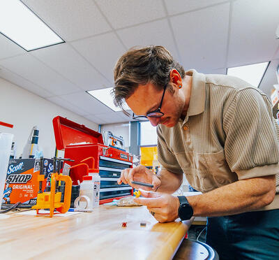
Long a partner of choice for the industry, the College of Engineering has grown up alongside it, evolving expertise in integrated circuit design, electronic materials and devices, process technology, packaging and integration, hardware security, artificial intelligence, and numerous sub-specializations. Together, these areas account for more than $12 million in annual research expenditures (about one-quarter of the college’s total) on projects involving some 45 faculty members and 200 graduate students.
The college has built long-lasting and mutually beneficial relationships with many leading tech companies in the region, including HP, one of the first towering giants of the Silicon Forest; Inpria, an Oregon State spinout acquired by JSR for $514 million in 2021; Analog Devices; and Lam Research, among others.
Oregon State was a major reason HP chose Corvallis when the company decided to expand outside of Silicon Valley in the mid-1970s. In the more than four decades since, HP has contributed millions of dollars to College of Engineering research, collaborated with faculty to create new materials and technologies, provided much-needed space on its Corvallis campus for university-affiliated research institutes and spinoff companies, and hired countless student interns and graduates. Today, about half of the company’s new college hires in Corvallis come from Oregon State.
Equipped for success
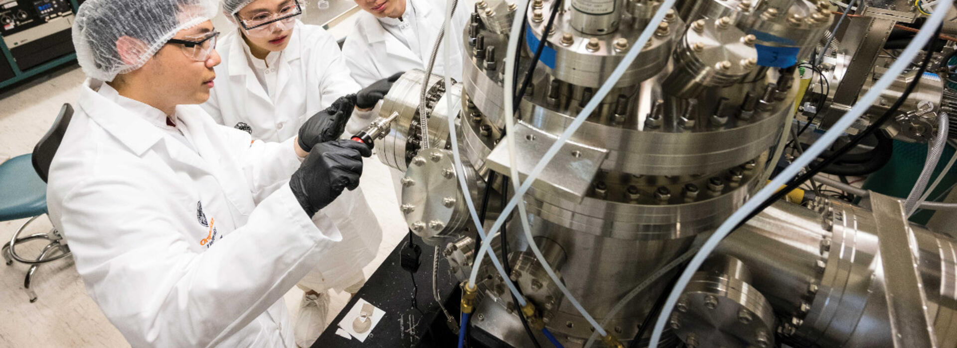
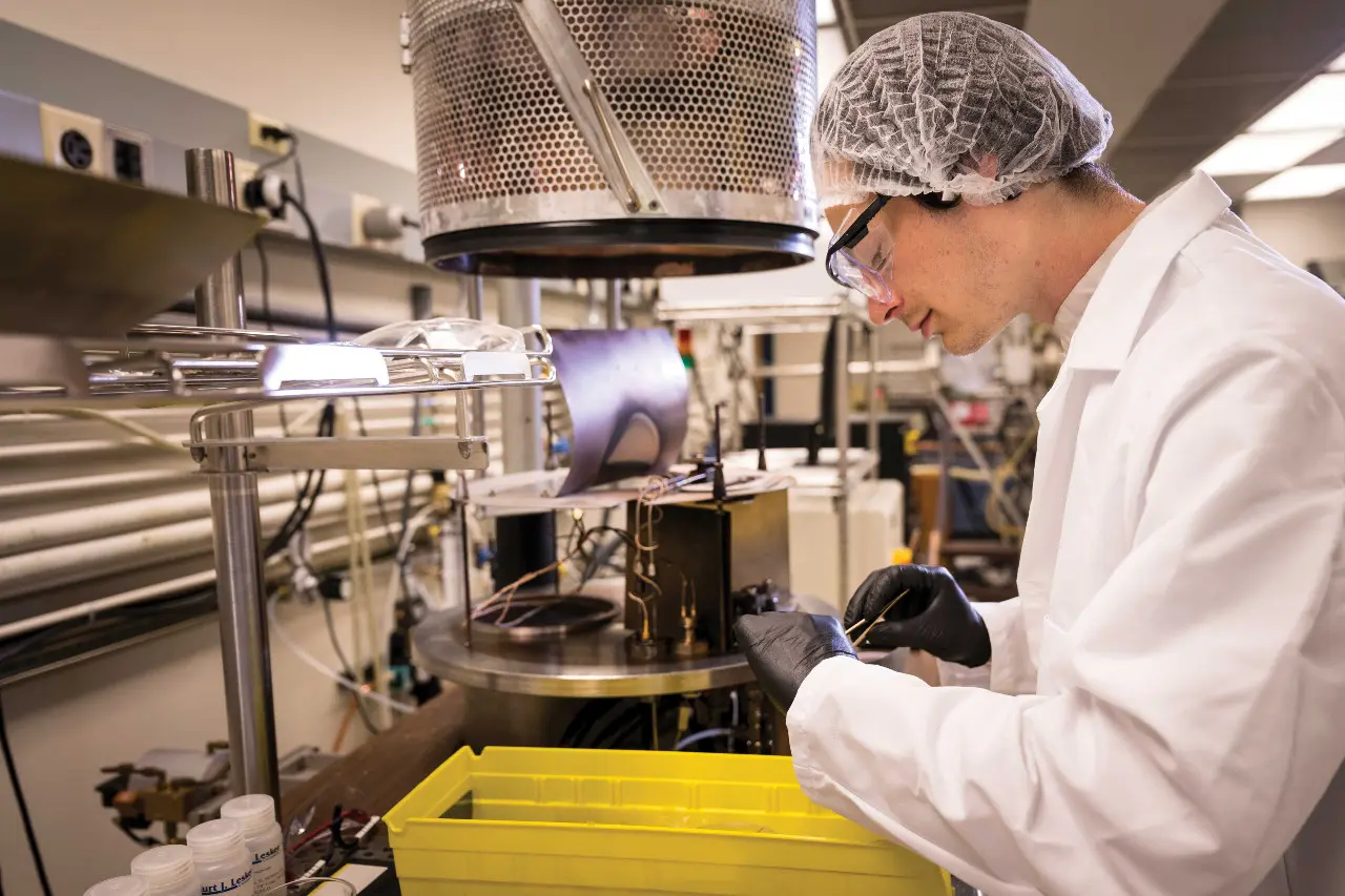
Over the years, Oregon State has established a number of specialized centers and institutes — often in collaboration with industry, peer institutions, and national laboratories — to drive continued innovation in semiconductor materials, design, and manufacturing. Two of these, the Advanced Technology and Manufacturing Institute and Oregon Nanoscience and Microtechnologies Institute, are housed in Building 11 on HP’s Corvallis campus.
The Northwest Nanotechnology Infrastructure site, created in 2015, and the Center for Design of Analog-Digital Integrated Circuits, which has operated since 1989, both were launched with funding from the National Science Foundation in partnership with other universities. In 2021, Oregon State launched the Oregon State Continuous Flow Facility, supported by the Murdock Charitable Trust and led by Douglas Keszler, Emeritus University Distinguished Professor of Chemistry.
Joining these facilities in 2025 will be the Huang Collaborative Innovation Complex. Designs for the $213 million, 150,000-square-foot complex are already underway, and construction could begin later this year. Notable features will include an NVIDIA supercomputer that promises to be among the most powerful at any university in the world.
Generational opportunity
“There’s a generational opportunity for federal funding, and we’re trying to position the university and the region in general to be as competitive as possible,” Weller said.
That opportunity announced itself last August, when President Joe Biden signed the bipartisan CHIPS and Science Act of 2022, a $52.7 billion package to accelerate domestic production of semiconductors, including $13 billion for research and workforce training.
Oregon leaders have responded in kind. In April of this year, Oregon Gov. Tina Kotek signed the Oregon Semiconductor and CHIPS Act. The Oregon spending bill leverages potential federal investment in Oregon’s semiconductor industry with $210 million in state funds, including $10 million to help public universities secure federal research grants. In June, the Oregon Legislature approved $72 million in state bonds to assist in the construction of the complex.
Regional Innovation Engines
In May, Oregon State was selected to spearhead a $1 million project, called Advancing Semiconductor Technologies in the Northwest, part of the NSF’s Regional Innovation Engines program. The effort is led by Pallavi Dhagat, professor of electrical and computer engineering. “The engine aims to partner with stakeholders in the region — industry, academic institutions, government laboratories, community outreach, and business development organizations and philanthropists — to develop a vibrant, inclusive, and sustainable ecosystem for education, research, and innovation in semiconductor technologies in the Pacific Northwest,” Dhagat said.
Oregon State will work with more than two dozen partners over the next two years, including the University of Washington, Boise State University, the Oregon Business Council, and the city of Hillsboro. At the conclusion of the project, the partners will be eligible for up to $160 million in additional funding over the succeeding 10 years.
The goals of the RIE include advancing use-inspired solutions for new and existing semiconductor materials and devices, inventing processes for scalable nanofabrication manufacturing, innovating energy-efficient, memory-centric computing architectures, increasing functionality via the More than Moore paradigm, developing innovative computation tools to better align co-design principles, expanding innovation and entrepreneurship, and supporting a diverse workforce by creating training programs and leveraging existing ones.
Northwest University Semiconductor Network
In June, Oregon State became a founding member of a university-industry collective tasked with developing the next generation of semiconductor workers. The Northwest University Semiconductor Network, led by Micron Technology Inc., will support research and experiential learning opportunities in the computer chip industry.
Micron and the universities in the network plan to align with a pair of industry groups, the American Semiconductor Academy and the SEMI Foundation, that are partnering on an initiative to build a comprehensive workforce development program through the combined efforts of universities, community colleges, and companies.
“Oregon State University is proud to be a founding member of Micron’s Northwest University Semiconductor Network and is committed to work with other regional universities and Micron to fully serve the technical needs and demands of the semiconductor industry and expand STEM access to underrepresented rural and urban students, including women,” said Oregon State University President Jayathi Murthy.
Oregon State and the other 12 founding partners were identified based on strong undergraduate and graduate programs in engineering and other STEM fields, their research and development expertise and the hands-on learning opportunities they provide.
More opportunities ahead
The College of Engineering is also key to several proposed industry-university partnerships that would further expand Oregon State research and technology transfer to the semiconductor industry.
Over the course of the spring term, faculty members submitted proposals for at least 15 CHIPS-related projects, totaling $47 million in potential research funding. These proposals include projects focusing on artificial intelligence hardware, next-generation wireless technology, and edge/IoT (Internet of Things) computing that would involve new collaborations with Fortune 100 partners as well a consortium of universities.
Most recently, the School of Chemical, Biological, and Environmental Engineering and the School of Electrical Engineering and Computer Science both received grants from Intel to develop curriculum related to sustainable semiconductor processing.
The leadership capital the College of Engineering is accruing through these efforts have the potential to carry over beyond the present-day needs of the semiconductor industry, Weller says.
“We really need to take advantage of this strategic opportunity for some big thinking in workforce development,” he said. “Today, we could be talking about semiconductors, where we happen to have the resources. But broadly speaking, we have major challenges in STEM ahead of us.”
Breakthrough in photonics
Researchers at Oregon State University and Baylor University have made a breakthrough in reducing the energy consumption of photonic chips used in data centers and supercomputers. Their innovation involves an ultra-energy-efficient method to compensate for temperature variations that degrade photonic chips. These chips will form the high-speed communication backbone of future data centers and supercomputers, according to John Conley, professor of electrical engineering and materials science, who co-led the Oregon State team.
“Our method is much more acceptable for the planet,” Conley said. “It will one day allow data centers to keep getting faster and more powerful while using less energy so that we can access ever more powerful applications driven by machine learning, such as ChatGPT, without feeling guilty.”
The circuitry in photonic chips uses photons, rather than electrons, to enable extremely rapid, energy-efficient transmission of data. The issue is that, until now, significant energy has been required to keep the chips’ temperature stable and performance high.
At present, the photonics industry relies on components known as “thermal heaters” to finetune the working wavelengths of high-speed, electro-optic devices and optimize their performance. These thermal heaters consume several milliwatts of electricity per device. While that may not sound like much, all of those milliwatts add up when multiplied by millions of devices.
The Oregon State team demonstrated that it’s possible to reduce the energy needed by a factor of more than 1 million by using gate voltage, which requires virtually no electric current, Conley said.
Centers and Institutes
ATAMI
The Advanced Technology and Manufacturing Institute (ATAMI) is home to College of Engineering faculty labs with a focus on advanced manufacturing processes, methods, and materials, and to the RAPID Manufacturing Institute for chemical process intensification. It provides a dynamic and highly collaborative environment with state-of-the-art tooling capabilities for faculty and private-sector partner tenants conducting research in advanced manufacturing processes, methods, and materials.
CDADIC
The Center for Design of Analog-Digital Integrated Circuits (CDADIC) is a leading university-industry partnership in its field. The center’s focus is innovative research in analog, RF, and mixed-signal IC design in collaboration with key industry partners. Analog-digital circuits have important applications across many fields, including communications, sensing, transportation, avionics and space technology, and medical technology.
MASC
The Materials Synthesis and Characterization (MASC) Facility is a comprehensive resource that serves as both an open user facility and an innovation center. MASC faculty and staff provide deep experience in thin-film deposition, device fabrication, and materials analysis. The facility serves as a hub for materials and device development on the Corvallis campus.
NNI
The Northwest Nanotechnology Infrastructure (NNI) site is a collaboration between the University of Washington and Oregon State University and is part of the National Science Foundation’s National Nanotechnology Coordinated Infrastructure. This site specializes in world-class nanotechnology infrastructure, paired with technical and educational leadership in integrated photonics, advanced energy materials and devices, and bio-nano interfaces and systems.