Introduction
Research in printed and flexible hybrid electronics (P-FHE) has led in recent years to the rapid expansion of innovative applications. Research funded by national sources, as well as leading tech companies, has underpinned growing outputs from Oregon State University. Additive manufacturing, the method used to create P-FHE, has seen specific advancements in ink substrates used in the manufacturing process. Further, a deeper understanding of 3D printers has allowed even more pioneering work in the field.
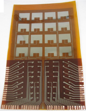
Unlike etching out of silicon, which is a subtractive method, additive manufacturing adds materials sequentially, eliminating waste and using lower-cost equipment. Several additive printing methods can be employed to produce P-FHE formats, including inkjet, screen, plasma jet, and gravure. Since devices can be printed at high rates with inexpensive equipment and with low material waste, the overall cost of P-FHE devices is significantly lower compared to traditional CMOS-based devices. Adding to that, abilities for flexibility, stretch, and bendability allow for novel applications and form factors not yet seen.
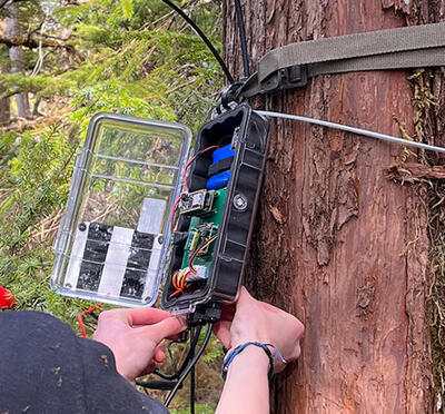
High-performance electronic devices that rely upon complementary metal-oxide semiconductor (CMOS) fabrication methods are usually performed inside foundries that house expensive equipment with ultralow-particle-count cleanrooms. While there are clear use-cases for these devices, not every application requires a high-performance chip to be integrated along with other high-performance components. Alternatively, P-FHE has been gaining a lot of traction recently owing to the rapid expansion of Internet of Things devices. These devices are especially suited for applications that require low-cost, low-medium performance metrics. Further, since these devices can be fabricated on flexible substrates, the devices have the advantages of being flexible, rollable, bendable, and stretchable.
The direct writing involved in the additive process opens up material and substrate choices, thereby enabling novel device applications. And while P-FHE devices won’t match the performance metrics of CMOS anytime soon, they can be complementary. For example, a device almost entirely manufactured in P-FHE form could connect to a traditional IC for increased processing power. Yet with flexible, high-performance, high-density flexible ICs already available, many P-FHE devices function quite well alone, satisfying the demand for moderate to low-performing requirements, as well as devices needing a nonrigid form.
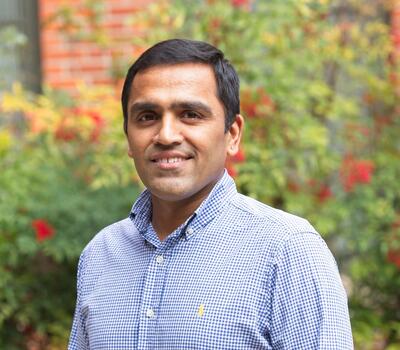
Research into P-FHE at Oregon State has been deepening with eight professors now firmly engaged. One of the standout leaders, Harish Subbaraman, assistant professor of electrical and computer engineering, was recently recruited to the College of Engineering for his pioneering work in P-FHE. Subbaraman heads a research group whose focus is on the development of novel materials systems compatible with various printers, the advancement of novel additive technologies for P-FHE development, the development and characterization of devices and systems with applications ranging from normal to extreme environments, and education and workforce development activities.
“After decades of promise, we are now seeing applications with NASA and other space agencies, where additive manufacturing technology coupled with P-FHE may finally allow for the exploration of deep space,” Subbaraman said. “In such a scenario, asteroids could be mined for raw materials, which could then be printed into flexible or rigid circuit form to replace or upgrade critical systems. Long ferry trips from Earth could be eliminated, effectively reducing risk and unleashing humanity to go much further than ever before.”
Subbaraman has been involved over the past 14 years in the advancement of printed electronics using four print modalities – inkjet printing, aerosol-jet printing, microdispenser, and plasma-jet printing.
“I have been involved in the first demonstrations of a fully-printed phased array antenna, a very high-frequency printed transistor, fully printed optical switches and modulators, radiation sensors, and electrochemical sensors,” Subbaraman said.
Subbaraman is a co-founder of INFlex Labs, whose aim is to commercialize printable inks. Products that he and his team have made available include multijet-compatible, low temperature-sinterable (~80-125 C) gold and platinum inks, and a variety of other metallic and 2D material inks possessing a variety of properties ranging from insulation to conductivity. Subbaraman believes the future is in these inks and how they can be leveraged to meet growing demand for interconnected electronic systems and data.
Based on his track record to date, Subbaraman and others have been invited into some high-profile, collaborative research projects with industry.
“There is significant interest in applying printing technologies for device development,” Subbaraman said. “For example, I am the principal investigator on a seed grant with HP, wherein we are looking at using plasma jet printers to selectively alter the properties of surfaces to achieve better adhesion control.”
With Moore’s Law under threat due to restrictions on bandwidth, power consumption, and integration density in traditional electronic circuit systems, the use of optical interconnects (vs. traditional electrical wiring) has the potential to solve these problems. Coupling chip-to-chip connections via optical connections with P-FHE devices presents another frontier where cost savings, reduced footprint, and flexibility may intersect.

The above image is a bar graph depicting the projected market size of flexible electronics from 2020 to 2030 in USD billions. Each bar represents one year, with a gradual increase in height as well as shades of blue (from light blue in 2020 to dark blue in 2030). The graph begins with $27.2 billion in 2020 and ends with $61 billion in 2030.
As with the printing press, where the cost of producing books plummeted and access soared as a result, an analogous path can be seen with P-FHE. With its flexible properties, P-FHE devices can be printed in roll-stock form, allowing thousands of circuits to be printed on a roll in minutes. And just imagine: We could have sensors, even biodegradable ones, keeping track of everything from the heavy metals in drinking water to stress hormone levels in babies. Cumbersome sensor packs weighing many pounds and taking up crucial space could be reduced to paper-thin, almost negligible form factors that save money and increase function. And, of course, let’s not forget deep space. The future is in P-FHE.
Looking ahead, Subbaraman noted that the College of Engineering is considering building a new center dedicated to P-FHE, due to the great deal of interest in the technology and its expected growth. An incredible talent pool is already in place, including a groundbreaking faculty and some excellent Ph.D. candidates.
To explore collaborative opportunities, or the semiconductor program in general, get in touch with us at: semi-osu@oregonstate.edu.