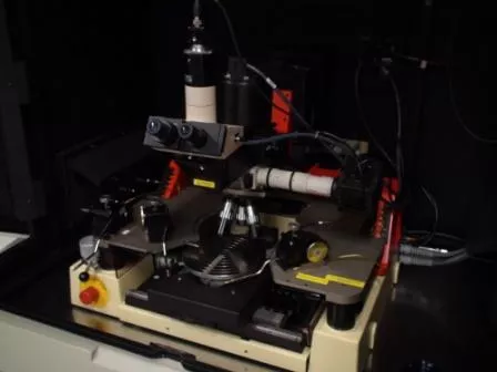
The dielectric testing station in the Owen characterization lab is used to characterize dielectric films.
Dielectric testing station
Owen Characterization lab

The micromanipulator testing station in the Owen characterization lab is used to characterize devices fabricated in the ECE 418 course.
Micromanipulator testing station
Probe Station
Owen Characterization lab

The REL 4800 station in the Owen characterization lab is used to characterize device.
Alessi
REL 4800
Probe station
Owen Characterization lab

This semiautomatic probe station has three Cascade Microtech DCM210 micropositioners with triaxial probe holders for use with an Agilent B1500A Semiconductor Device Analyzer, and two Alessi MH series micropositioners with coaxial probe holders for use with an Agilent 4284A Precision LCR Meter. The probe station accommodates up to 8” wafers. It is equipped with a dark box and vibration isolation table.
Karl Suss
PA200 Semiautomatic Probe System with Agilent B1500A SDA and Agilent 4284APrecision LCR meter
Semiautomatic probe station with dark box, semiconductor device analyzer and LCR meter
Owen Characterization lab

This manual probe station is used to measure IV characteristics of thin film devices. Four positioners, two Micromanipulator Model 110 and two Model 210, are available to make contact to features on the order of 50um square. The long working distance Model 6400 microscope includes lenses with magnification of 2.25x, 8x and 25x. Measurements are taken with the Agilent 4156C Precision Semiconductor Parameter Analyzer.
The Micromanipulator Company, Inc.
6000 Series Test Station with Agilent 4156CPrecision Semiconductor Parameter Analyzer
Manual probe station with dark box and semiconductor parameter analyzer
Owen Characterization lab